We Love To Explore New CHALLENGES.
PCB design brings electronic circuits to life in the physical form. Use of layout software in PCB design helps to combine component placement and routing for defining electrical connectivity on a manufactured circuit board. Typical PCB design process includes: component placement, PCB routing, ECAD-MCAD integration, and final design. PCB design complexity is categorized into low-end, medium end, and high-end.
During the whole design cycle, we continuously interact and get confirmations from customers before proceeding to the next phase of design process. We make sure that the development is carried out in conformity with IPC standards.
We have the experience required to consistently meet the highest standards in the industry. Our experience spans multiple market segments, including Telecom, Datacom, Computer & Storage, Medical, Industrial, and consumer products
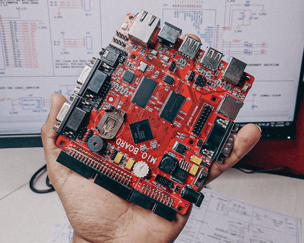
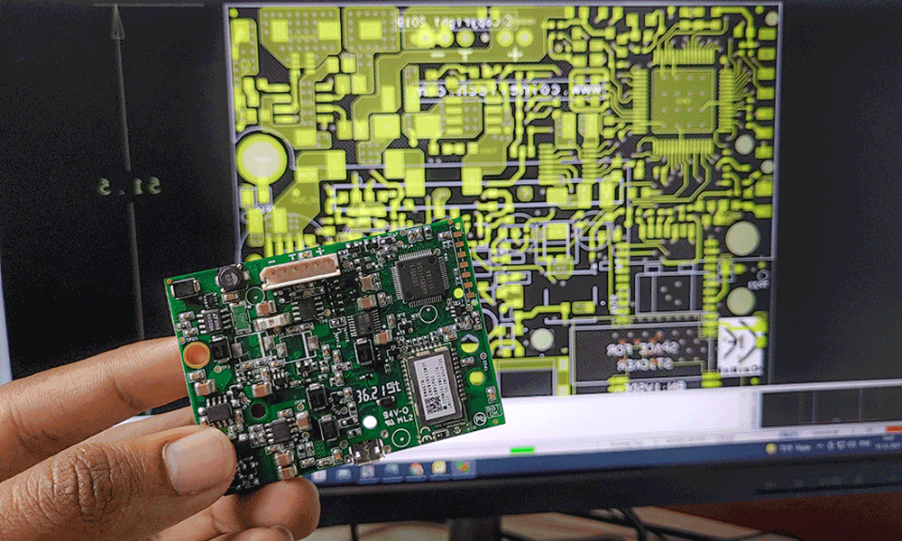

PCB Designs Of Any Level Of Complexity
- Design various types of PCB:Construction 3D models Impedance controlled Designs with delay matching, Stack-up and material selection.
- Analog, digital, high-frequency.
- Single-sided, double sided and multi layer printed-circuit-boards.
- Multilayer printed circuit boards with BGA-packages, with blind and buried vias.
- Multiple Fine pitch BGA (0.5mm) of high pin count per chip (512).
- Analysis of signal integrity (SI)
- Analysis of electromagnetic compatibility (EMC)
- Assistance in PCB manufacture and mounting.
To start working on a PCB design we require from the customer minimal initial data in the form of electric circuit scheme, the list of components and requirement specifications.Creation of component libraryWe form component libraries as per JEDEC or IPC norms as applicable.
Preliminary configuration for Board Layout
We arrange the components according to the requirement specifications provided, fix components with rigid arrangement. According to the possibilities/requirements we can make a proposal for changing PCB dimensions. At this stage we can provide the client with a design image for conforming design requirements by dimensions and component placement parameters. Implicit requirements (additional plug connectors, additional test points or test sockets, etc.) are discussed and changes are done as required.
Board Design
We perform final placement of elements, optimize connections, set traces parameters and layout rules, define number of layers and perform trace routing (wiring). If required, we can calculate characteristic and differential impedance. If necessary, we can model transient phenomena in circuits, analyze signal integrity, electromagnetic compatibility (EMC), thermal modes.
Verification
Company’s technical experts perform additional control which minimizes the probability of mistakes.
Acceptance
We finalize and transfer the complete set of the design documentation in conformity with customer’s requirements. As a result the customer receives:
- The project file in the appropriate design environment;
- Files for PCB manufacture (Gerber 274-X, CAM350);
- The complete set of the PCB design documentation including mounting drawing, specification and PCB drawing according to the customer’s requirements.
Design and modeling environments
Our specialists have skills in using the following packages and environments:
- CADENCE.SPB 15.7 and above (OrCAD, Allegro)
- KiCAD
your IDEAs come to life
CoiNel is a firm believer of getting it right the first time. We have techniques to ensure all the entrapped errors are corrected before the product is brought to you. Thus saving your time, cost and a frustratingly vicious cycle of incorrect outputs & alterations to rectify it.
Our design services comes with great success rates and we follow all well known and good design practices to ensure there are no mistakes and hence your products can enter market faster.