
LPC2148 DEV Board
₹300.00 – ₹2,000.00
Description
OVERVIEW
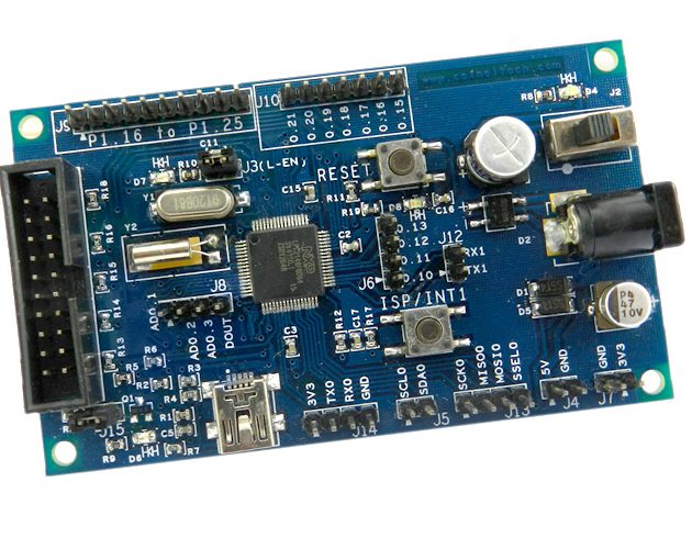
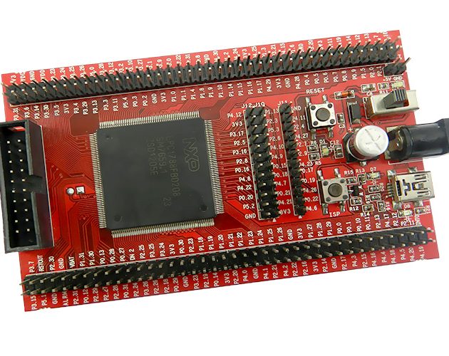
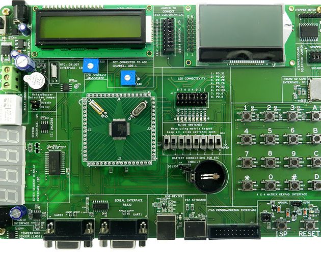
LPC2148 DEV Board is an extension board for LPC2148 Header Board with ARM7 core microcontroller (LPC2148). The DEV Board is a cost effective solution for learning and designing applications based on ARM7 core. The DEV Board has numerous peripheral connectivity options thereby making it easy for the user to kickstart with firmware development using this board. All the source codes that demonstrate working of each of the onboard modules/peripherals are provided along with the board.
The graphical display connectivity option is available for the following display units.
Graphical LCD Connectivity Options
- Model: TM12864H6CCGWA-1
- Driver IC: ST7567S
- Data Interface Parallel
- Number of Pixels: 128 x 64
- Display Module Size: 74 x 39 mm
- Driver IC: ST7567S
- Model: TM12864A8CCWGWA
- Driver IC: ST7565R
- Data Interface Parallel
- Number of Pixels: 128 x 64
- Display Module Size:52.40 x 77.40 mm
This Graphical Display is not the part of the package. You can also purchase the graphical LCD separately from the following link
TM12864H6CCGWA-1 Graphical LCD
TM12864A8CCWGWA Graphical LCD
Features of LPC2148 Dev Board
- Processor: NXPs ARM7 TDMI LPC2148.
- Clock:
-
- 12MHz for CPU
- 32.768 KHz for RTC
- Interfaces
-
- SD Card through SPI
- PS2 Connectivity Option
- USB Device.
- UART (UART0 and UART1) in RS232 options.
- Graphical LCD Connectivity Option (Can be used as GPIO)
- 4×4 Keypad connectivity Option (Can be used as GPIO)
- I2C Based four, common anode 7 Segment Display.
- 16 x 2 alphanumeric LCD with HD44780 driver.
- RTC with CMOS Battery Backup.
- POT via ADO.1
- 256 Kb EEPROM (I2C)
- Temperature Sensor (LM35) via ADO.2
- Audio through DAC output.
- Buzzer, Test LED, Relay
- On Board Reset and ISP
- Power by USB and/or adaptor.
- 20 PIN standard JTAG Connectivity
- Pinout for 5V and 3.3V
- Manual and Auto ISP programming Options.
- Board Dimensions: 138 x 123 mm
- Board Specifications:
-
- Laminate: FR4
- Board Thickness: 1.6mm
- Finish: ENIG
Kit Deliverables:
- ARM7 LPC2148 Dev Board
- USB Cable.
JTAG Options for Debug/Programming:
Parallel Port JTAG (tested on Keil, Rowley CrossWorks)
CoiNel ARM USB JTAG (tested on Rowley CrossWorks)
The Board can also be used with other JTAG Debuggers (Check compatibility to ensure).
The details on how to use the JTAG and its associated plugins are provided with the documents and also can be downloaded from Download and Support sections.
ISP Programming:
Programming can be done through the on chip boot loader using UART interface (UART0). You will have to use a TTL to RS232 Converter to do so since the pinout are TTL logic and PC uses RS232 logic. The tool used for programming is Flash Magic
USB Boot Loader:
The Board can also be programmed via USB Secondary Bootloader. Check the document for LPC2148 USB Boot Loader for more details.
TOOLS:
Our products can be used with majority of IDE and plugins that support ARM7 LPC21xx family. A few IDE and plugin details are given below.
- Keil uvision4 IDE (32K code limited version can be used.)
- Rowley Crossworks(30 day evaluation version can be used.)
- IAR workbench (32K code limited version could be used.)
- GCC based open source tool chains
Plugins/Programmers:
H-JTAG, Flash Magic have been tested.
Compatible debuggers like U-Link, J-Link etc can also be used.
LPC2148 MCU Specifications
- High Performance 32-bit ARM7TDMI-S™ CPU with 512 Kb Flash.
- 32 KB Data Memory (SRAM).
- In-System Programming/In-Application Programming (ISP/IAP) via on-chip boot loader software.
- Single Flash sector or full chip erase in 400 ms and programming of 256 bytes in 1 ms.
- Embedded ICE RT and Embedded Trace interfaces offer real-time debugging with the on- chip Real Monitor software and high-speed tracing of instruction execution.
- USB 2.0 Full-speed compliant device controller with 2 KB of endpoint RAM.
- Provides 8KB of on-chip RAM accessible to USB by DMA.
- Two 10-bit ADCs provide a total of 14 analog inputs, with conversion times as low as 2.44 us per channel.
- Single 10-bit DAC provides variable analog output.
- Two 32-bit Timers/External event counters.
- Four Capture and four Compare channels.
- PWM unit with six output pins.
- Low power Real-time clock with independent power and dedicated 32 kHz clock input.
- Multiple serial interfaces including two UARTs, two Fast I2C (400 kbit/s), SPI™ and SSP with buffering and variable data length capabilities.
- Up to 45 of 5 V tolerant general purpose I/O pins.
- Up to nine edge or level sensitive external interrupt pins.
- On-chip integrated oscillator operates with external crystal in range of 1 MHz to 25 MHz.
- Power saving modes include Idle and Power-down.
- Individual enable/disable of peripheral functions.
- Processor wake-up from Power-down mode via external interrupt.
- Single power supply chip with Power-On Reset (POR) and Brown-Out Detection (BOD)
- CPU Operating Voltage range of 3.0 V to 3.6 V
Related products
Reviews
There are no reviews yet.